- 您现在的位置:买卖IC网 > Sheet目录2008 > MAX1183ECM+TD (Maxim Integrated Products)IC ADC 10BIT 40MSPS DL 48-TQFP
MAX1183
Dual 10-Bit, 40Msps, 3V, Low-Power ADC with
Internal Reference and Parallel Outputs
_______________________________________________________________________________________
3
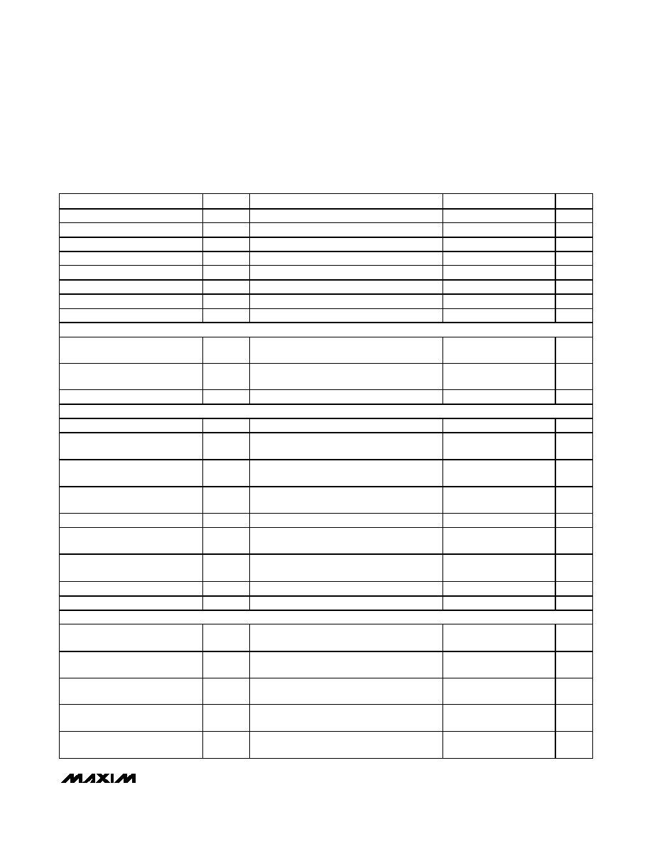
ELECTRICAL CHARACTERISTICS (continued)
(VDD = 3V, OVDD = 2.5V, 0.1F and 1.0F capacitors from REFP, REFN, and COM to GND, REFOUT connected to REFIN through a
10k resistor, VIN = 2VP-P (differential with respect to COM), CL = 10pF at digital outputs (Note 1), fCLK = 40MHz, TA = TMIN to TMAX,
unless otherwise noted. Typical values are at TA = +25°C.) (Note 2)
PARAMETER
SYMBOL
CONDITIONS
MIN
TYP
MAX
UNITS
Small-Signal Bandwidth
Input at -20dBFS, differential inputs
500
MHz
Full-Power Bandwidth
FPBW
Input at -0.5dBFS, differential inputs
400
MHz
Aperture Delay
tAD
1ns
Aperture Jitter
tAJ
2psRMS
Overdrive Recovery Time
For 1.5 x full-scale input
2
ns
Differential Gain
±1
%
Differential Phase
±0.25
Degrees
Output Noise
INA+ = INA- = INB+ = INB- = COM
0.2
LSBRMS
INTERNAL REFERENCE
Reference Output Voltage
REFOUT
2.048
±3%
V
Reference Temperature
Coefficient
TCREF
60
ppm/
°C
Load Regulation
1.25
mV/mA
BUFFERED EXTERNAL REFERENCE (VREFIN = 2.048V)
REFIN Input Voltage
VREFIN
2.048
V
Positive Reference Output
Voltage
VREFP
2.012
V
Negative Reference Output
Voltage
VREFN
0.988
V
Differential Reference Output
Voltage Range
VREF
VREF = VREFP - VREFN
0.95
1.024
1.10
V
REFIN Resistance
RREFIN
>50
M
Maximum REFP, COM
Source Current
ISOURCE
5mA
Maximum REFP, COM
Sink Current
ISINK
-250
A
Maximum REFN Source Current
ISOURCE
250
A
Maximum REFN Sink Current
ISINK
-5
mA
UNBUFFERED EXTERNAL REFERENCE (VREFIN = AGND, reference voltage applied to REFP, REFN, and COM)
REFP, REFN Input Resistance
RREFP,
RREFN
Measured between REFP and COM and
REFN and COM
4k
Differential Reference Input
Voltage Range
VREF
VREF = VREFP - VREFN
1.024
±10%
V
COM Input Voltage Range
VCOM
VDD/2
±10%
V
REFP Input Voltage
VREFP
VCOM +
VREF/2
V
REFN Input Voltage
VREFN
VCOM -
VREF/2
V
发布紧急采购,3分钟左右您将得到回复。
相关PDF资料
MAX1184ECM+TD
IC ADC 10BIT 20MSPS DL 48-TQFP
MAX1186ECM+TD
IC ADC 10BIT 40MSPS DL 48-TQFP
MAX1187CCUI+
IC ADC 16BIT 135KSPS 28-TSSOP
MAX118EAI+
IC ADC 8BIT 1MSPS 28-SSOP
MAX1191ETI+T
IC ADC 8BIT 7.5MSPS DL 28-TQFN
MAX1192ETI+T
IC ADC 8BIT 22MSPS DL 28-TQFN
MAX1195ECM+TD
IC ADC 8BIT 40MSPS DL 48-TQFP
MAX1197ECM+TD
IC ADC 8BIT 60MSPS DL 48-TQFP
相关代理商/技术参数
MAX1183ECM-D
功能描述:模数转换器 - ADC RoHS:否 制造商:Texas Instruments 通道数量:2 结构:Sigma-Delta 转换速率:125 SPs to 8 KSPs 分辨率:24 bit 输入类型:Differential 信噪比:107 dB 接口类型:SPI 工作电源电压:1.7 V to 3.6 V, 2.7 V to 5.25 V 最大工作温度:+ 85 C 安装风格:SMD/SMT 封装 / 箱体:VQFN-32
MAX1183ECM-TD
功能描述:模数转换器 - ADC RoHS:否 制造商:Texas Instruments 通道数量:2 结构:Sigma-Delta 转换速率:125 SPs to 8 KSPs 分辨率:24 bit 输入类型:Differential 信噪比:107 dB 接口类型:SPI 工作电源电压:1.7 V to 3.6 V, 2.7 V to 5.25 V 最大工作温度:+ 85 C 安装风格:SMD/SMT 封装 / 箱体:VQFN-32
MAX1184ECM
制造商:Maxim Integrated Products 功能描述:DUAL 10-BIT, 20MSPS, +3V, LOW-POWER ADC WITH - Rail/Tube
MAX1184ECM+D
功能描述:模数转换器 - ADC 10-Bit 2Ch 30Msps High Speed ADC RoHS:否 制造商:Texas Instruments 通道数量:2 结构:Sigma-Delta 转换速率:125 SPs to 8 KSPs 分辨率:24 bit 输入类型:Differential 信噪比:107 dB 接口类型:SPI 工作电源电压:1.7 V to 3.6 V, 2.7 V to 5.25 V 最大工作温度:+ 85 C 安装风格:SMD/SMT 封装 / 箱体:VQFN-32
MAX1184ECM+TD
功能描述:模数转换器 - ADC 10-Bit 2Ch 30Msps High Speed ADC RoHS:否 制造商:Texas Instruments 通道数量:2 结构:Sigma-Delta 转换速率:125 SPs to 8 KSPs 分辨率:24 bit 输入类型:Differential 信噪比:107 dB 接口类型:SPI 工作电源电压:1.7 V to 3.6 V, 2.7 V to 5.25 V 最大工作温度:+ 85 C 安装风格:SMD/SMT 封装 / 箱体:VQFN-32
MAX1184ECM-D
功能描述:模数转换器 - ADC RoHS:否 制造商:Texas Instruments 通道数量:2 结构:Sigma-Delta 转换速率:125 SPs to 8 KSPs 分辨率:24 bit 输入类型:Differential 信噪比:107 dB 接口类型:SPI 工作电源电压:1.7 V to 3.6 V, 2.7 V to 5.25 V 最大工作温度:+ 85 C 安装风格:SMD/SMT 封装 / 箱体:VQFN-32
MAX1184ECM-T
制造商:Maxim Integrated Products 功能描述:DUAL 10-BIT, 20MSPS, +3V, LOW-POWER ADC WITH - Tape and Reel
MAX1184ECM-TD
功能描述:模数转换器 - ADC RoHS:否 制造商:Texas Instruments 通道数量:2 结构:Sigma-Delta 转换速率:125 SPs to 8 KSPs 分辨率:24 bit 输入类型:Differential 信噪比:107 dB 接口类型:SPI 工作电源电压:1.7 V to 3.6 V, 2.7 V to 5.25 V 最大工作温度:+ 85 C 安装风格:SMD/SMT 封装 / 箱体:VQFN-32